


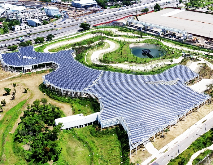
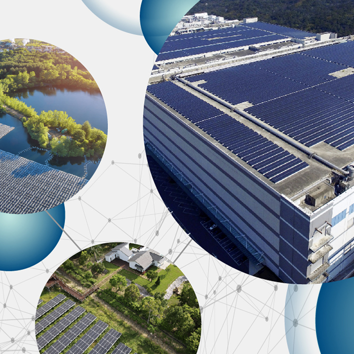
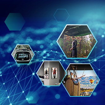
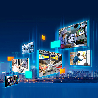
Smart Vertical Solutions for Limitless Possibilities
By integration of technical expertise and market insights, we provide our partners with access to smart solutions that stride beyond today’s cutting edge for new opportunities in retail, education, enterprise, healthcare, mobility, manufacturing, and energy sectors.


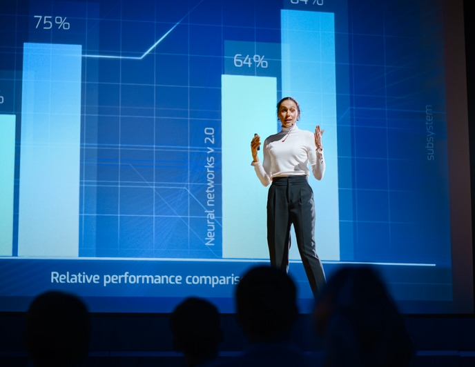
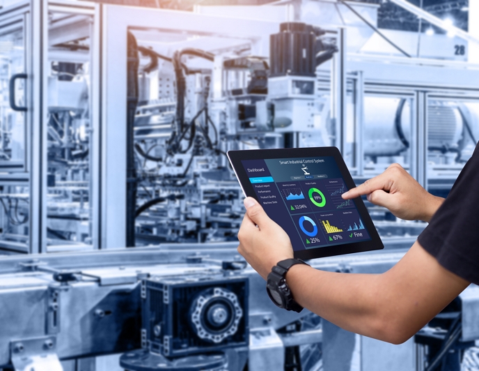

Technical Expertise


Our Advantages
We provide technical expertise and diversified solutions to open up new opportunities for our partners. We drive mutual success to attain the shared vision by our competences in flexible manufacturing, sustainable supply chain, global operation, and group synergy.
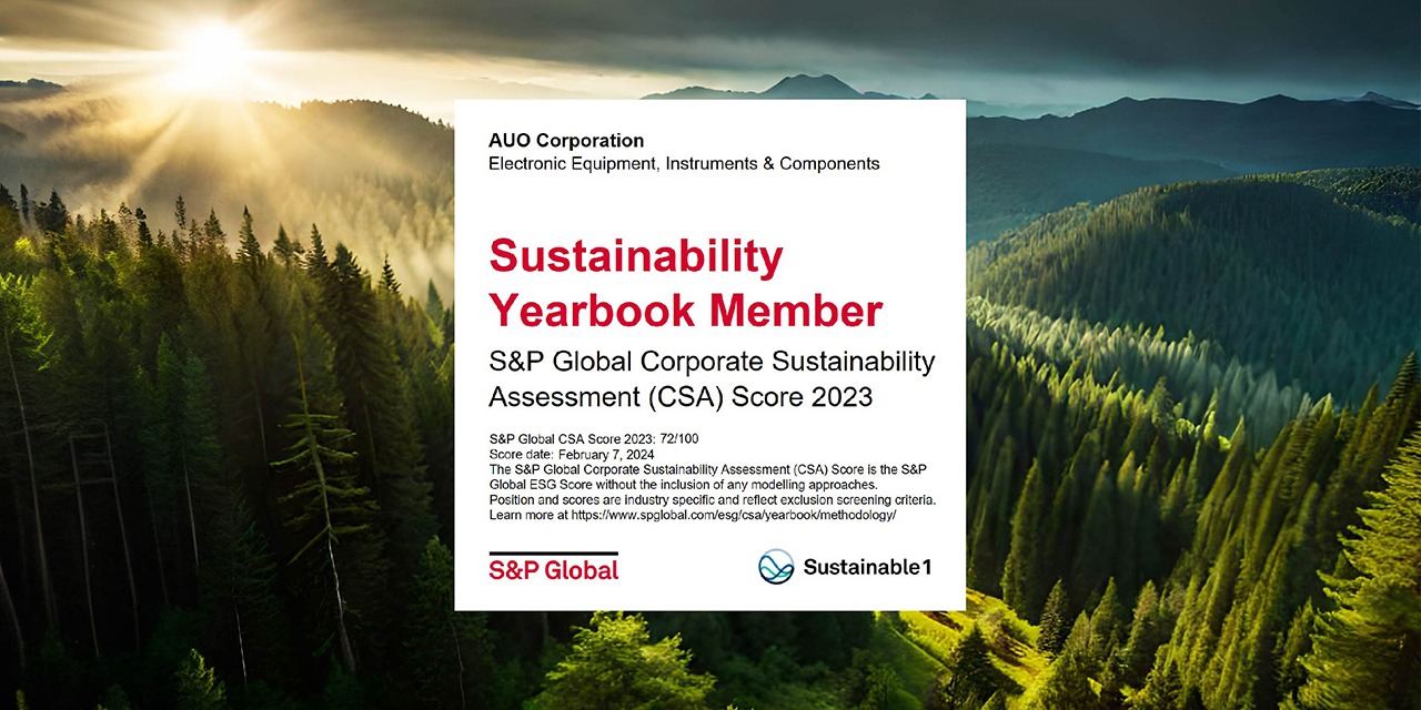
13
Years for DJSI Inclusion
Top
100
Clarivate Innovators & LexisNexis Innovation Momentum Inclusion
31,000
Submitted Patent Applications


Connections with AUO Group
-
Learn how we shape the future with our innovations and smart solutionsWant to know more? We are here to help!